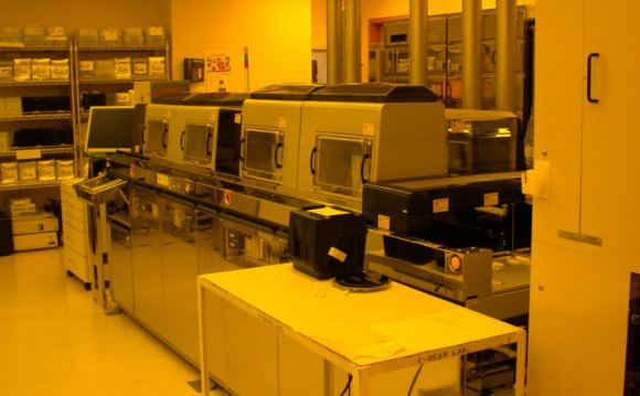
 Interconnect requirements for the 22nm technology node and beyond, driven by shrinking FEOL geometry, push the limits of unit process tools for BEOL as well as FEOL. BEOL tools for WLCSP (Wafer level chip scale packaging) take advantage of many lithographic techniques utilized in the manufacture of the chip in the Front End of Line (FEOL).
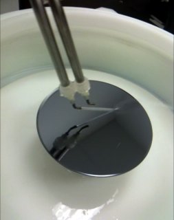
One of the principal processes utilized in the back end of line is the Photolithographic process to perform such steps as redistribution layer, under bump metallization, and bump formation. An example of bump formation during the lift-off resist process is shown below:
Semiconductor photolithographic processing steps are discussed below.
 Wafer Handling steps
- The substrate is automatically withdrawn from a cassette which may be in a SMIF pod. Alternatively for 300mm wafers a FOUP opener may be employed.
- The substrate is precisely positioned on a rotatable vacuum chuck such that the center of the substrate is coincident with the center of rotation of the vacuum chuck.
- After photoresist is applied the substrate is baked (normally on a heated plate provided for the purpose.)
- The substrate is returned to the cassette or to a second cassette.
Photoresist coating steps
- Pre-Wet Dispense – The substrate is rotated at a speed of approximately 500 rpm and a pre-wet dispense using the same solvent used in the photoresist, normally NMP or PGMEA is briefly dispensed and “spun” off at a speed of about 1500 rpm.
 The purpose of this step is to remove any dust particles from the wafer surface that could affect the quality of the deposited film and to effectively pre-wet the surface of the wafer with a monolayer of solvent molecules so that the surface can more readily accept the photoresist. This also has the effect of reducing the quantity of photoresist that needs to be applied thereby reducing chemical costs. The small quantity of solvent used is more than compensated by the reduced quantity of photoresist required.
 - Coating. The rotational velocity of the substrate is maintained at
about 1500 rpm and the photoresist is dispensed at the center of the wafer for about 1 second. It is important that this be done immediately after the last Newton ring of solvent has evaporated.
- Spinning – The rotational velocity of the substrate is increased to the speed at which the desired photoresist thickness is obtained. This speed will be highly dependent upon the resist viscosity. The acceleration to achieve the desired velocity will be on the order of 4, 000 to 8, 000 rpm per second. Precise control of both the acceleration and the velocity will determine the uniformity of the film thickness within a given substrate, from substrate to substrate and lot to lot.
Share this Post
latest post
-
-
-
 History of advertising Photography October 10, 2016
 -
 Materials for pinhole camera October 7, 2016
 -
 Photojournalism photographers October 4, 2016
 -
 35mm nitrate film October 1, 2016
 -
 Photographic films September 28, 2016
 -
 One Colour Photographs September 25, 2016
 -
 Best compact digital camera for street photography September 22, 2016